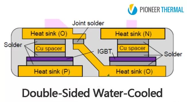
An IGBT module consists of IGBT chips and FWD chips. The sur m of the power losses from these sections equals the total power loss for the module. Power loss can be cla assified as either on-state loss or switching loss. A diagram of the power loss factors is shown as follows.

The on-state power loss from the IGBT and FWD sections can be calculated using the output characteristics, while switching loss can be calculated from switching loss vs. collector current characteristics. Use these power loss calculations in order to design cooling sufficient to keep the junction temperature Tj below the maximum rated value. The on-voltage and switching loss values to be used here, are based on the typical junction temperature Tj (125°C or 150°C are recommended). For characteristics data, refer to the module specification sheets.


 +86-18902844286
 E-mail
